SIOM Studies Deep-Ultraviolet Subwavelength Aperture Diffraction
上海光机所在深紫外亚波长小孔衍射研究方面取得进展
Topics and contents
Topic
On this page
The Shanghai Institute of Optics and Mechanics (SIOM) has made progress in deep-ultraviolet subwavelength aperture diffraction research, supporting lithography inspection.
The source article provides specific data and details that help assess actual progress in this direction
Excellent Innovation Center for Intense Laser Science Briefing
(Issue 818)
August 25, 2026
SIOM Makes Progress in Deep-Ultraviolet Subwavelength Pinhole Diffraction Research
Recently, a team led by Researcher Li Sikun in the High-End Optoelectronic Equipment Department of the Shanghai Institute of Optics and Fine Mechanics (SIOM), Chinese Academy of Sciences, made progress in deep-ultraviolet subwavelength pinhole diffraction research. The related results, titled "Vector diffraction modeling and parametric study of 266 nm sub-wavelength pinholes for high-NA wavefront sensing", were published in Applied Optics.
In high-end optical equipment such as lithographic projection objectives, mask inspection, wafer defect inspection and laser direct writing, wavefront measurement accuracy directly affects system performance. Shack-Hartmann wavefront sensors and point diffraction interferometers typically use pinhole diffraction to generate a reference wave that is nearly an ideal sphere. According to diffraction principles, reducing the pinhole diameter improves the wavefront quality and numerical aperture of the reference wave, but also makes fabrication more difficult and lowers energy transmission. Under deep-ultraviolet conditions at a wavelength of 266 nm and high numerical aperture, the vectorial nature of light, polarization effects and waveguide modes inside the pinhole cannot be ignored, and conventional scalar diffraction theory can no longer accurately describe the pinhole's energy coupling and far-field wavefront characteristics.
To address these issues, the research team developed a full-vector electromagnetic simulation model combining the generalized Richards-Wolf vectorial focusing integral, the three-dimensional finite-difference time-domain method (3D-FDTD), and near-to-far-field transformation. The model sequentially performs high-numerical-aperture focused field generation, near-field solution for a subwavelength aperture, and far-field wavefront reconstruction; the overall modeling workflow is shown in Figure 1. Building on this, the researchers systematically analyzed the effects of aperture diameter and thickness, incident numerical aperture, typical initial aberrations, and sidewall tilt errors on energy transmittance, output numerical aperture, energy uniformity, and wavefront root-mean-square error.
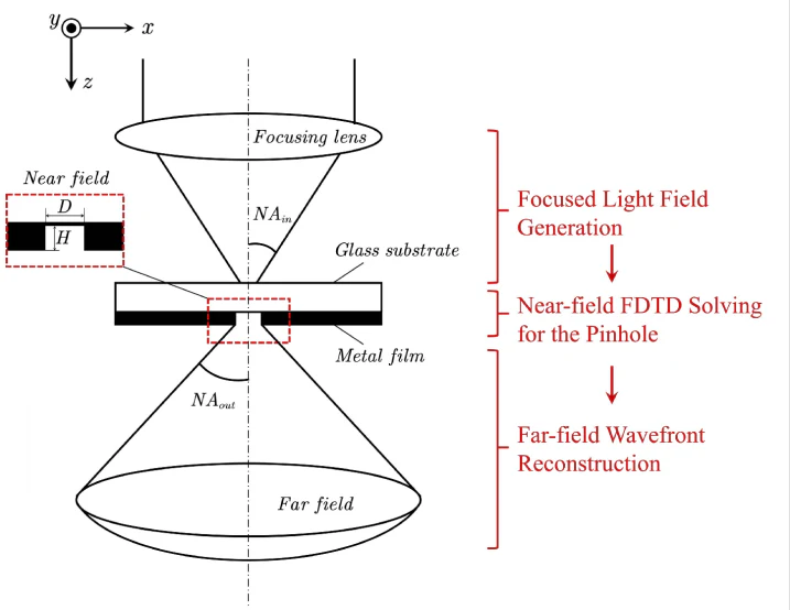
Figure 1 Schematic of the full-vector aperture diffraction model for high-numerical-aperture wavefront sensing at a 266 nm wavelength
The results show that aperture diameter is the main factor determining far-field wavefront quality, while aperture thickness modulates the diffracted wave through longitudinal resonance and waveguide-mode cutoff. The researchers selected two sets of typical aperture parameters and compared the near-field distributions inside the apertures, as shown in Figure 2. The results reveal distinct standing-wave patterns inside the apertures, with different diameters corresponding to different longitudinal resonance states, causing the energy transmittance to vary non-monotonically. A two-dimensional parameter sweep of aperture diameter and thickness was then performed, with results shown in Figure 3. The aperture energy transmittance exhibits a striped distribution with diameter and thickness, mainly arising from constructive and destructive interference caused by Fabry-Perot-like longitudinal resonances inside the aperture; over a thickness range of about 100–160 nm, resonance can increase wavefront distortion, whereas further increasing the thickness allows waveguide-mode cutoff to suppress higher-order modes and improve wavefront purity.
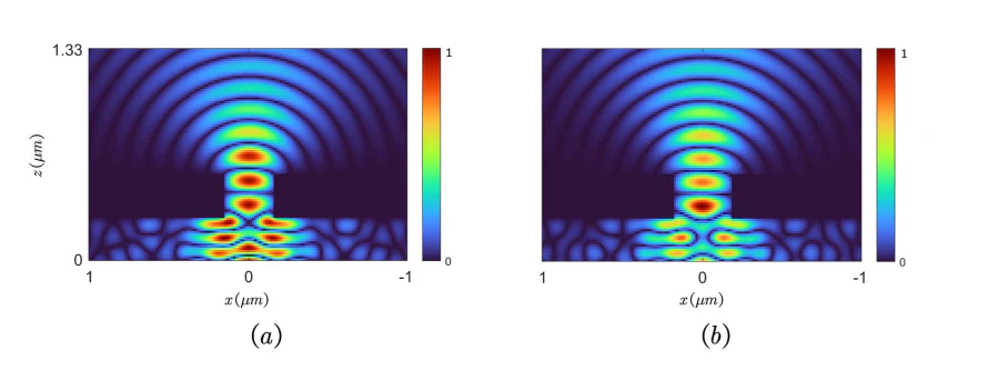
Figure 2 Near-field distributions inside the aperture and longitudinal resonance characteristics for different aperture diameters.(a)Smaller diameter; (b)Larger diameter.
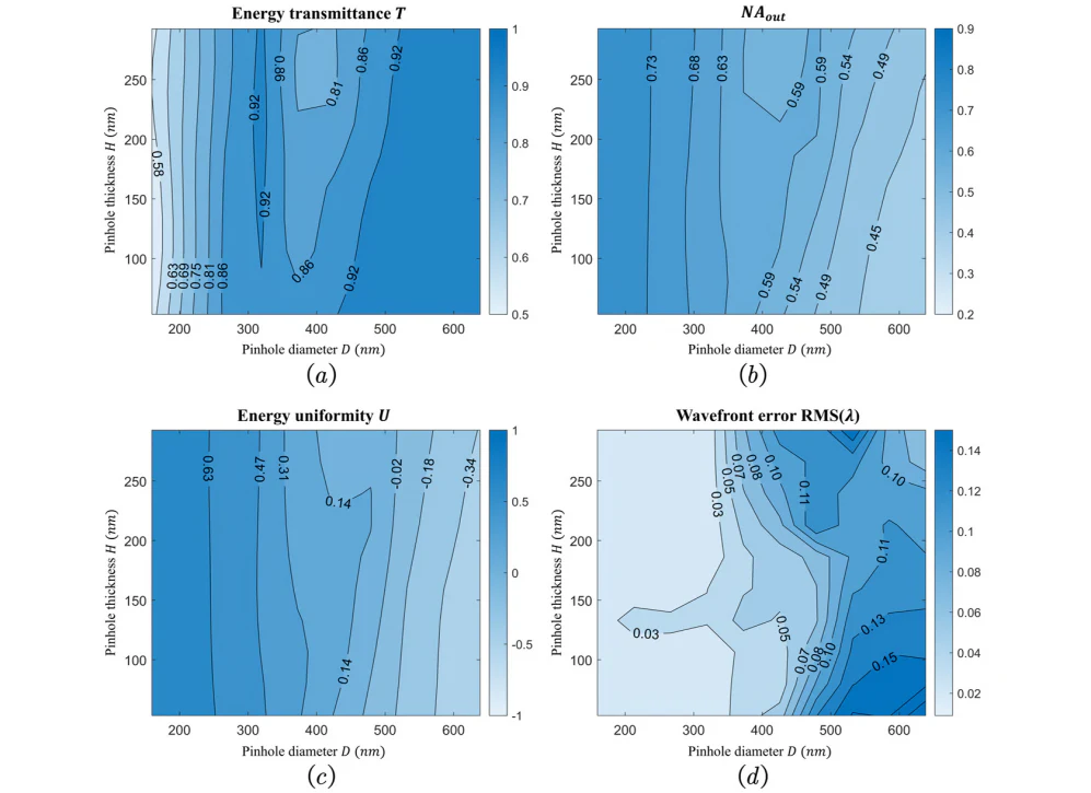
Figure 3 Combined effects of aperture diameter and thickness on different metrics.(a) Energy transmittance; (b) Output NA; (c) Energy uniformity; (d) Wavefront error RMS.
The researchers further examined the combined effect of aperture diameter and incident numerical aperture, with results shown in Figure 4. The study divides the aperture's operating regimes into a “diffraction-dominated region” and a “geometric projection region.” When the aperture diameter is below 350 nm, output wavefront quality and wide-angle diffraction characteristics are governed mainly by the aperture size and are highly robust to changes in incident numerical aperture. Within the model and parameter ranges of this study, an incident numerical aperture above 0.2 provides a good balance between energy transmittance and wavefront quality; specifically, with an aperture diameter below 350 nm, it is possible to simultaneously achieve an energy transmittance above 0.6, an output numerical aperture above 0.6, and a wavefront root-mean-square error below 0.05λ. When the aperture diameter increases beyond 400 nm, the aperture increasingly acts as a geometric stop; increasing the incident numerical aperture raises the output numerical aperture but introduces significant wavefront distortion. The study also found that the actual output numerical aperture deviates markedly from predictions by the conventional scalar formula, indicating that engineering designs cannot rely solely on empirical formulas to determine aperture size.
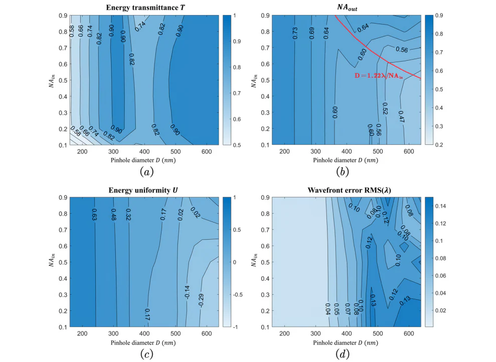
Figure4 Joint effect of pinhole diameter and incidentNAon different metrics.(a) Energy transmittance; (b) outputNA; (c) energy uniformity; (d) wavefront errorRMS.
In addition, the study shows that subwavelength pinholes have strong spatial filtering capability for rotationally symmetric or even-symmetric aberrations such as spherical aberration and astigmatism, while being more sensitive to coma, which breaks the central symmetry of the optical field. For the sidewall tilt commonly encountered in practical fabrication, slight tapering within the85°—90°range does not cause significant performance degradation, and at around86°both energy transmittance and wavefront quality can be improved simultaneously. This study establishes a systematic parameter map and numerical design guidelines for266 nmsubwavelength pinholes, providing a theoretical basis for the design of deep-ultraviolet high-precision wavefront sensing reference sources. The study currently relies mainly on a perfect conductor model; future work will further incorporate the dispersion characteristics and ohmic losses of real metals such as aluminum and chromium.
Source: Shanghai Institute of Optics and Fine Mechanics (SIOM) · Research Updates · siom.cas.cn