Guangyin Technology Unveils 8×8 Nanosecond-Scale OCS
光引科技发布8×8纳秒级OCS,推动光交换走向近计算侧
Topics and contents
Guangyin Technology has launched an 8×8 nanosecond-scale optical circuit switch, bringing optical switching closer to the compute side.
On September 9, the 27th China International Optoelectronic Exposition (CIOE 2026) opened at the Shenzhen World Exhibition & Convention Center. Guangyin Technology, which focuses on optoelectronic integration chips and modules, presented its three business segments—optical sensing, optical switching, and optical computing—and officially launched an 8×8 nanosecond-scale Optical Circuit Switching (OCS) product for AI data centers.
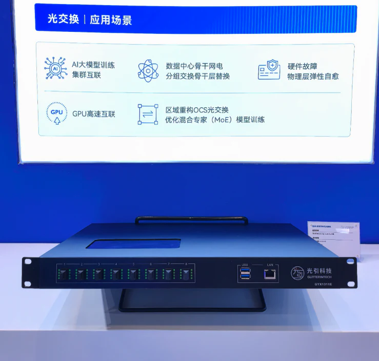
8X8 nanosecond-scale OCS developed by Guangyin Technology
During the exhibition, Guangyin Technology CTO Yan Ting was invited to give a keynote on "nanosecond optical switching," systematically explaining the trend of AI networks moving from relatively static connections to dynamic organization, the application boundaries of OCS at different speed tiers, and the technical value and industrialization path of nanosecond-scale optical switching moving further toward the compute side.
Compute clusters move from fixed interconnects to dynamic compute networks
As AI large-model training and inference scales continue to expand, communication demands within compute clusters are undergoing profound changes. In particular, with new architectures such as Mixture-of-Experts (MoE), different tokens are dynamically assigned to different experts, and communication peers, traffic directions, and bandwidth requirements shift constantly with the computing task. Compared with traditional AI models, network traffic is becoming more dynamic, bursty, and highly parallel.
Guangyin Technology believes that in scale-up interconnects, network capabilities can be understood along two key dimensions: transmission determines whether data can arrive fast enough, while switching determines where data should flow and how bandwidth is organized. The former continues to drive the development of high-speed optical I/O, while the latter is opening up new space for OCS; together, they determine how much effective compute an AI cluster can ultimately deliver.
OCS can establish end-to-end optical paths directly in the optical domain, reducing per-packet processing at intermediate switching nodes and unnecessary optical-electrical-optical conversions, while reconfiguring physical links according to compute and communication needs. Large-port-count OCS based on MEMS technology is better suited to large-scale connections across racks and clusters, as well as relatively infrequent resource provisioning and topology adjustments. As OCS moves further inside the rack and closer to compute units such as GPUs, however, communication cycles keep shrinking, traffic patterns change more frequently, and GPUs become more sensitive to network latency, making switching speed increasingly critical.
This also means that OCS devices operating at different speeds are not simple substitutes for one another; instead, they address needs at different layers and time scales within AI networks.
8×8nanosecond-scaleOCS brings optical switching to finer-grained compute cycles
In the upper layers of data center networks, connectivity is relatively stable, and millisecond- or microsecond-scale OCS can already handle fault rerouting, resource allocation, and lower-frequency network topology adjustments. But the closer to the GPU, the shorter the communication cycles and the higher the synchronization frequency, and the more readily any extra waiting time introduced by the network translates directly into GPU idle time.
For near-compute deployments, this raises a more fundamental question for OCS: can optical switching be fast enough for network reconfiguration to truly operate on the time scale of computation and communication?
The 8×8 OCS unveiled this time by Guangyin Technology uses silicon photonic integrated switching technology to push optical path switching into the nanosecond range. Compared with OCS mainly serving lower-frequency resource provisioning and topology adjustments, the significance of nanosecond-scale OCS lies not merely in "switching faster," but in moving optical switching from network resource provisioning toward compute scheduling, allowing physical connections and bandwidth between GPUs to be adjusted rapidly in step with task and traffic changes.
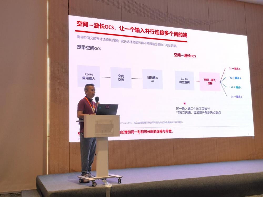
Guangyin Technology CTO Yan Ting Delivers Keynote on OCS
According to system-level research by the Guangyin Technology team on near-compute interconnects, under 400G links and corresponding workloads, the system begins to show clear performance gains once effective network reconfiguration time reaches roughly the 200-nanosecond range. As per-link rates rise further from 400G to 800G and even 1.6T, data transfer cycles shorten further, placing higher demands on network reconfiguration speed.
In practice, when communication demands among a group of GPUs change, the underlying network can adjust connections and bandwidth more quickly. In MoE models, traffic between different experts shifts with token routing, giving the network more flexibility to match compute workloads and reducing the time GPUs spend waiting for data and communication synchronization, thereby raising the cluster's effective compute throughput.
"AI workloads are becoming increasingly dynamic. In the future, networks cannot simply allocate resources once before a task begins; they must gradually gain the ability to adjust connectivity and bandwidth as computing tasks change," said Yan Ting. "The significance of nanosecond optical switching is that it pushes OCS from relatively low-frequency network resource allocation closer to the compute side, giving optical switching a chance to enter the finer-grained cadence of computing and communications."
On the chip R&D front, Guangyin Technology has already developed a nanosecond-scale integrated OCS with 16×16 dimensions. The release of this 8×8 nanosecond-scale OCS product marks an important step in advancing the technology from chip validation toward module- and system-level applications. Future products will undergo system validation in scenarios including high-speed GPU interconnects, MoE inter-expert communication scheduling, bandwidth reallocation in AI training and inference clusters, and rapid link switching in the event of hardware failures.
Yan Ting also stressed that optical switching is not intended to fully replace electrical switching. Electrical switching offers mature store-and-forward, packet processing and congestion management capabilities and remains a key foundation of modern data center networks. A more realistic direction going forward is a hybrid optoelectronic switching architecture combining OCS with electrical switching: electrical switching handles complex packet processing and control functions, while OCS provides more direct and efficient optical connections on specific high-bandwidth, low-latency links.
One Optoelectronic Integration Platform Extending Sensing, Connectivity and Computing
During the exhibition, Guangyin Technology also presented its latest advances in optical sensing and optical computing.
In optical sensing, the company has launched a portable skin spectroscopy device based on its in-house micro-spectrometer chip, capable of accurately measuring skin collagen, moisture and oil levels. It continues to drive the commercialization of spectral sensing technology in consumer electronics, industrial inspection and other scenarios.
In optical computing, Guangyin Technology continues to develop programmable photonic processors and novel optical-domain computing architectures, exploring the high parallelism, low latency and high energy efficiency of light to offer new computing pathways for future matrix operations, intelligent vision, network control and edge computing.
Optical sensing, optical switching and optical computing are not three independent technology systems. They share underlying capabilities such as optoelectronic integrated chip design, programmable photonic devices, packaging testing and control algorithms, with tailored product solutions formed for different applications.
From sensing the physical world, to connecting computing resources, to participating in information processing, Guangyin Technology is using optoelectronic integrated chips at its core to continuously expand the application boundaries of light in the intelligent era, gradually turning its vision of "empowering chips with light" into scalable products and solutions. 
Source: C114 Communications Network · Optical Communications · c114.com.cn