Shanghai Institute of Optics and Fine Mechanics Achieves Deep-Subwavelength Long-Wave Infrared Absorption and Thermal Emission Control
上海光机所在深亚波长长波红外吸收/辐射调控研究方面取得进展
Topics and contents
A team at the Shanghai Institute of Optics and Fine Mechanics has proposed and demonstrated a lithography-free Cr/a-GST/Bi planar metal-insulator-metal absorber based on ultrahigh-refractive-index materials. With a total thickness of only 550 nm, it achieves high absorption and thermal emission control across the 8-14 μm long-wave infrared band.
The original work presents a lithography-free, ultrathin long-wave infrared absorber structure that is relevant to infrared stealth and thermal management devices
Shanghai Institute of Optics and Mechanics Reports Progress in Deep-Subwavelength Long-Wavelength Infrared Absorption/Thermal Emission Control
Recently, a team from the High-Power Laser Component Technology and Engineering Department at the Shanghai Institute of Optics and Fine Mechanics, Chinese Academy of Sciences, made new progress in deep-subwavelength long-wavelength infrared absorption and thermal emission control. The team proposed and experimentally demonstrated a lithography-free Cr/a-GST/Bi planar metal-insulator-metal (MIM) absorber based on giant-refractive-index materials. With a total thickness of only 550 nm, it achieves broadband, high-efficiency absorption across the long-wavelength infrared (LWIR, 8-14 μm) atmospheric window, while offering large-angle and polarization-insensitive operation. The work, titled “Deep-subwavelength long-wavelength infrared absorber enabled by giant-refractive-index materials for thermal bolometer and camouflage,” was published in Optics Express.
The long-wavelength infrared band overlaps strongly with the dominant thermal emission band of objects at room temperature, making it highly valuable for infrared thermal imaging, infrared sensing and thermal camouflage. Practical applications require absorbers that combine high absorptance, broadband response, angular and polarization stability, ultrathin thickness and scalable fabrication. Conventional LWIR meta-absorbers largely rely on lithographically patterned lateral micro- and nano-resonant structures, which are complex and costly to fabricate and difficult to manufacture over large areas; their absorption performance is also easily affected by the incident angle and polarization state. Developing LWIR absorbers that need no complex patterning while remaining ultrathin, broadband and optically robust therefore remains a challenge.
To address these issues, the team designed the intrinsic optical properties of the materials in concert with a planar optical cavity, introducing giant-refractive-index bismuth (Bi) and the high-index, low-loss amorphous Ge2Sb2Te5 (a-GST) material. In the LWIR band, the real part of the refractive index of Bi is close to 10, while that of a-GST is about 3.7. The researchers built a planar MIM optical cavity from 40 nm Bi, 410 nm a-GST and 100 nm Cr, with no lateral micro/nano patterning or lithographic processing. Experimental results show a peak absorptance of 97.0% at 9.6 μm, with a full width at half maximum of about 5.6 μm. Layer-resolved absorption analysis further shows that, at 9.6 μm, more than 85% of the incident light energy is dissipated within the 40 nm thick Bi layer, whereas a free-standing Bi film of the same thickness absorbs only about 27%—indicating that the high-efficiency absorption stems from the synergy between the giant-refractive-index Bi and the MIM optical cavity. The device maintains strong, stable absorption as the incident angle increases to 70°; at 60° oblique incidence, switching polarization from TE to TM changes the 9.6 μm absorptance by only about 5%, demonstrating good angular and polarization robustness.
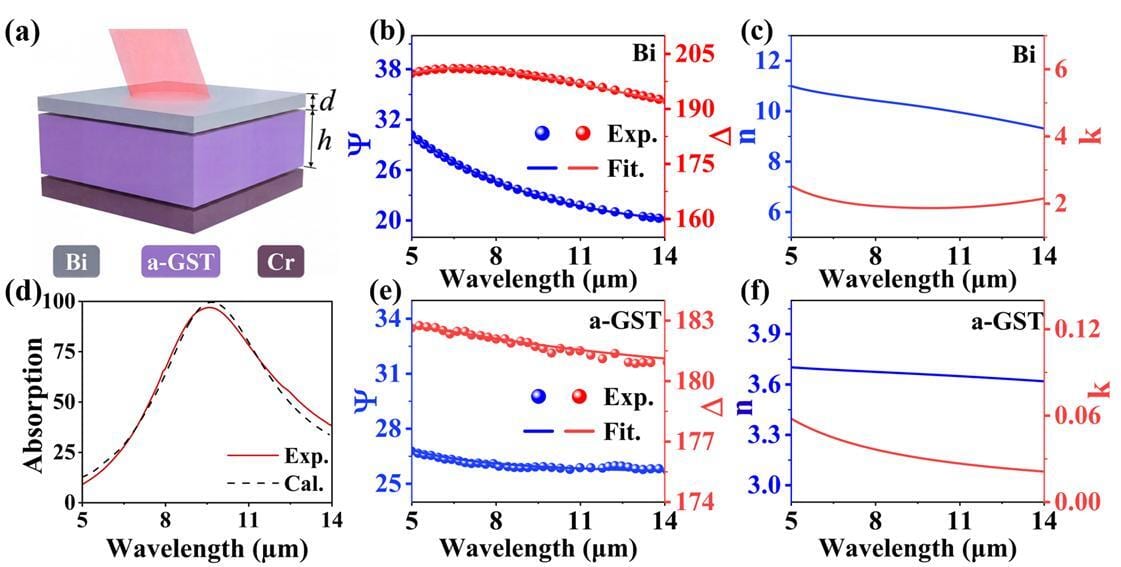
Figure 1. Cr/a-GST/Bi planar MIM deep-subwavelength LWIR absorber: structure, optical constants of the materials, and experimental/theoretical absorption spectra.
Building on its ultrathin profile, high absorption and Bi-dominated energy dissipation, the team further explored the device's potential for uncooled infrared microbolometers and thermal camouflage. The Bi film has a temperature coefficient of resistance (TCR) of about -0.30% K⁻¹; finite-element thermal simulations show that when the Bi layer rises by 10 K, the underlying Cr layer rises by only about 0.2 K, indicating that the a-GST spacer effectively suppresses heat diffusion into the substrate. Meanwhile, the device has an average emissivity of about 0.77 over the 8-13 μm band and a peak emissivity above 0.99 near 9.6 μm. LWIR imaging experiments showed that, against a high thermal-emission background such as a human hand, the sample exhibited weak infrared thermal contrast with the surrounding skin, confirming its passive thermal camouflage capability. The study offers new material and structural design ideas for low-cost, large-area uncooled infrared detection and multifunctional thermal emission control devices.
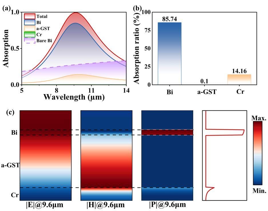
Fig.2. Layer-resolved absorption and electromagnetic field distribution of the Cr/a-GST/Bi MIM absorber. (a) Total absorption spectrum and absorption contributions from the Bi, a-GST, and Cr layers; (b) absorption fractions of each layer at 9.6 μm; (c) normalized electric field, magnetic field, and time-averaged power dissipation density distributions at 9.6 μm.
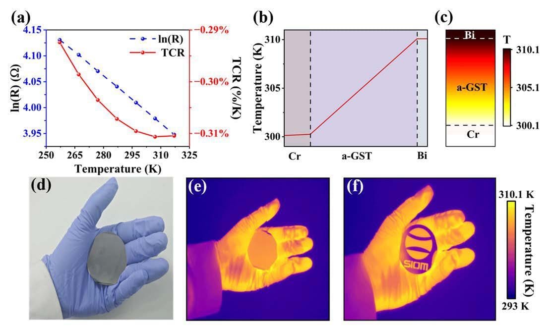
Fig.3. Thermoresponsive performance, thermal localization simulation, and long-wave infrared imaging results of the device.
This work was supported by the National Natural Science Foundation of China, the Natural Science Foundation of Shanghai, and the China Association for Science and Technology Young Talent Support Program, among other projects.
Source: Shanghai Institute of Optics and Fine Mechanics (SIOM) · Research Updates · siom.cas.cn