SIOM Fabricates Large-Area, Wide-Angle, Broadband AR Metasurface Using Nanoimprint Lithography
Topics and contents
A team from the Department of High-Power Laser Component Technology and Engineering at the Shanghai Institute of Optics and Fine Mechanics (SIOM) used nanoimprint lithography to fabricate large-area, double-sided fused-silica nanopillar metasurfaces, achieving broadband, wide-angle antireflection from the visible to near-infrared, along with good high-temperature stability and laser damage tolerance.
The original article provides a scalable nanoimprint process and laser damage tolerance, offering practical value for high-power laser optics
Shanghai Institute of Optics and Mechanics Reports Progress in Large-Area, Wide-Angle, Broadband Antireflective Metasurfaces
Recently, a team from the High-Power Laser Component Technology and Engineering Department at the Shanghai Institute of Optics and Fine Mechanics, Chinese Academy of Sciences, made new progress in large-area, wide-angle, broadband antireflective metasurfaces. The team used nanoimprint technology to fabricate large-area, double-sided fused-silica nanopillar metasurfaces, achieving broadband, wide-angle antireflection from the visible to the near-infrared, along with good high-temperature stability and laser damage tolerance. The results were published in Applied Physics Letters under the title “Large-area nanoimprinted metasurfaces for wide-angle broadband antireflection with refractory and laser durability”.
High-power laser optics must combine low reflectance, high thermal stability and a high laser-induced damage threshold. Conventional multilayer antireflection coatings offer excellent spectral performance, but their multiple interfaces are prone to thermal stress, cracking or delamination under high temperatures and intense laser light, and their antireflection performance is sensitive to incidence angle and polarization. Bio-inspired "moth-eye" subwavelength structures reduce Fresnel reflection through a graded refractive index, offering broadband and wide-angle advantages. However, achieving large-area, high-fidelity double-sided patterning on fused silica while maintaining high-temperature stability and laser durability remains challenging.
To address these issues, the team combined nanoimprint lithography with inductively coupled plasma etching to fabricate tapered nanopillar arrays about 190 nm high on both sides of a 2 × 2 cm2 fused-silica substrate. This single-material graded-index structure reduced the average reflectance of the silica from 5.6% to below 2.4% across 400-1500 nm, while providing wide-angle antireflection with low polarization dependence. The nanostructures also improved surface wettability. After annealing at 1100 ℃, the structural morphology and spectral performance remained essentially stable; in nanosecond laser tests at 1064 nm, the laser-induced damage threshold was estimated at 23.5 J/cm2. The study demonstrates double-sided fused-silica nano-metasurfaces that combine broadband, wide-angle antireflection, high-temperature stability and high laser durability, offering a new fabrication approach for high-power laser optics.
This work was supported by the National Natural Science Foundation of China, the Natural Science Foundation of Shanghai, and the China Association for Science and Technology Young Talent Support Program, among other projects.
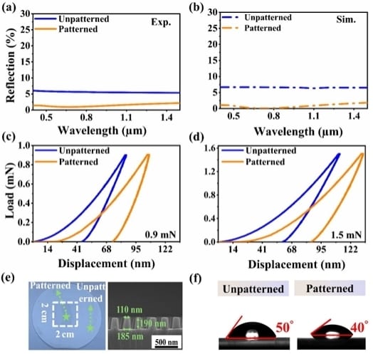
Figure1. Optical performance and structural characterization of the large-area double-sided fused silica nanopillar metasurface. (a) Measured and (b) simulated reflection spectra of unpatterned and patterned samples; (c)-(d) nanoindentation test results; (e)2 × 2 cm2 sample photograph and SEM image of the nanopillar structure; (f) water contact angles of unpatterned and patterned samples.
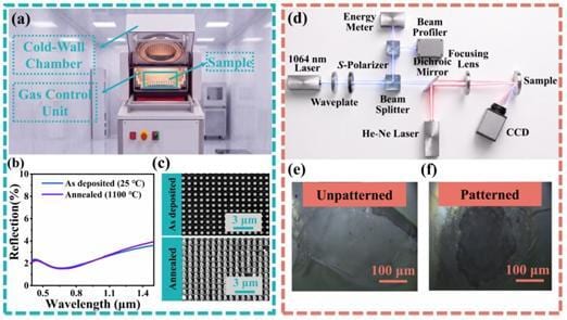
Figure2. High-temperature stability and laser damage characteristics of the large-area fused silica nanopillar metasurface. (a) Rapid thermal processing setup; (b)1100 ℃ reflection spectra before and after annealing; (c) SEM images before and after annealing; (d)1064 nm nanosecond laser damage test setup; (e)-(f) typical laser damage morphologies of unpatterned and patterned samples.
Source: Shanghai Institute of Optics and Fine Mechanics (SIOM) · Research Updates · siom.cas.cn