Silicon Carbide Joins the Mass-Production Race as a Next-Generation Material for AR Optics
Topics and contents
Silicon carbide AR waveguides are moving toward wafer-level manufacturing and small-volume production, but low-cost, high-volume consumer shipments remain some way off. A recent preprint from the Zhejiang Provincial Key Laboratory of 3D Micro/Nano Fabrication and Characterization, the Institute of Optoelectronics at Westlake University, and the Mude Micro-Nano team presents a full-color silicon carbide diffractive waveguide measuring 0.35 mm thick and weighing 1.98 g, with patterning of four pairs of lenses demonstrated on an 8-inch SiC wafer. The high refractive index helps widen the field of view and enable monolithic full color, but manufacturing challenges remain, including consistency of optical-grade substrates, micro- and nanofabrication of hard and brittle materials, and light leakage at packaging interfaces.
Starting from the field-of-view and monolithic full-color advantages of high refractive index, this article reviews the mass-production constraints of silicon carbide waveguides across substrates, micro- and nanofabrication, and packaging.
AROptical Materials Silicon Carbide: Where Exactly Is the Bottleneck?
By Duan Jiaxu
Edited by Shanzi
Recently, a paper preprint jointly released by the Zhejiang Provincial Key Laboratory of 3D Micro-Nano Fabrication and Characterization, the Westlake Institute of Optoelectronics, and Mude Micro-Nano presented a full-color silicon carbide diffractive waveguide just 0.35mm thick and weighing only 1.98g.
The paper also presents a wafer-level fabrication process compatible with nanoimprint lithography, enabling patterned fabrication of four pairs of lenses on an 8-inch SiC wafer. Compared with the 0.75mm, 3.795g design announced in 2025, the SiC waveguide takes another step toward lighter weight and scalable manufacturing.
This has brought SiC, a material route previously associated mainly with semiconductors and new energy vehicles, back into the spotlight for AR displays.
In fact, SiC did not enter AR only recently. Meta Orion has already thrust SiC optical waveguides into the industry spotlight, and a growing number of research teams and companies in China and abroad are now developing SiC waveguides. Why is everyone studying SiC, and how will it change AR displays in the future?
The answer starts with the material properties of SiC itself.
Why SiC?
Silicon carbide (SiC) is a compound material made of silicon and carbon. It is also a typical wide-bandgap semiconductor (SiC, GaN and other third-generation semiconductor materials offer high voltage tolerance, low conduction loss and good thermal conductivity).
Its uses are extremely broad. Early on, people valued its durability: silicon carbide can be used as an abrasive in grinding wheels and cutting discs, or made into ballistic ceramics for bulletproof vests. In high-performance cars such as Ferrari and Lamborghini, carbon-fiber-reinforced silicon carbide composites are also used to make carbon-ceramic brake discs.

With the advent of the semiconductor era, people began to exploit its high voltage tolerance, high temperature resistance and good thermal conductivity to manufacture devices such as power MOSFETs and Schottky diodes. In more advanced directions, SiC is also gradually entering research fields such as integrated photonics, quantum networks and spin qubits.

These seemingly very different applications make one thing clear: SiC has distinctly defined material properties. It is hard, heat resistant and highly stable.
SiC has a Mohs hardness of about 9 to 9.5, second only to diamond. It also has high thermal conductivity and a low coefficient of thermal expansion, so it does not deform significantly even under abrupt temperature changes.
In optics, however, another standout property is prized: its high refractive index.
In 2024, Meta publicly adopted SiC diffractive optical waveguides in Orion, thrusting this previously niche material route into the AR industry spotlight.
SiC is used in AR optical displays mainly in diffractive optical waveguides.
Put simply, a diffractive optical waveguide creates nano-scale grating structures on the lens surface to couple light into the waveguide, change its direction of propagation and ultimately guide it to the eye. During this process, the light can travel several centimeters through a thin lens thanks to another fundamental optical phenomenon: total internal reflection.

When light travels from a high-refractive-index material into a lower-index medium, such as from glass into air, the refracted ray hugs the interface ever more closely as the angle of incidence increases. Once the angle of incidence exceeds a certain critical value, light no longer exits the material and is instead reflected entirely back into it. This is total internal reflection.
That critical value is known as the "critical angle." Because different materials have different refractive indices, the critical angle for total internal reflection also varies. The higher the refractive index, the smaller the critical angle, which means light at a wider range of angles can be "trapped" and guided inside the waveguide.
Here is a demonstration:
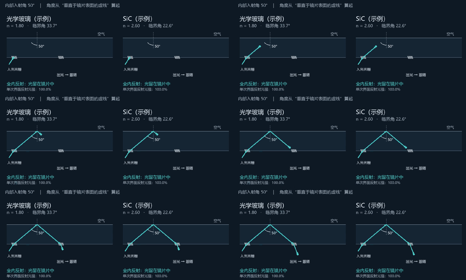
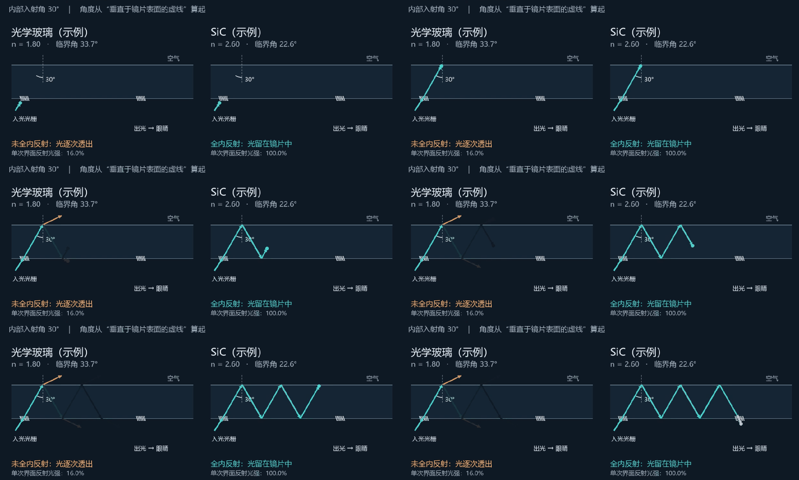
The highest refractive index glass can currently achieve is 2.0. To push further, researchers continue to search for better materials. Enter SiC, with a refractive index of 2.6.
This is also one of the key reasons Meta chose SiC. Orion ultimately achieved a field of view of about 70 degrees, while some simulations show that, under the same design conditions, a glass substrate with a refractive index of 2.0 has a theoretical FOV limit of about 35 degrees, whereas SiC can reach 80 degrees.
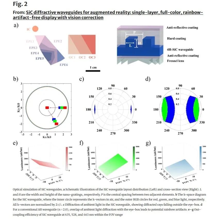
Another potential advantage of a high refractive index is single-waveguide full color.
In conventional full-color diffractive waveguides, red, green and blue light at different wavelengths propagate at different angles after passing through the grating. To keep all three colors stably guided, some designs use two or even three waveguide layers to handle the colors separately.
SiC's higher refractive index, by contrast, gives RGB light a wider angular margin, making it realistic to integrate all three colors in a single waveguide. In 2025, Westlake University and other teams demonstrated a monolithic, full-color SiC diffractive waveguide with no rainbow effect.
That is why SiC with a refractive index of 2.6 is, in theory, a true next-generation material capable of driving major advances in several of the most critical AR glasses issues at once: field of view, full-color display and slimmer, lighter headsets.
A great material, but also a hard nut to crack
Friends who often play God may know that when God opens a window for you, the door is usually shut. SiC may look "perfect" in every respect, but the fact that it was not deployed at scale earlier means there are certainly tough problems to overcome.
The most fundamental issue is that SiC for AR has different material requirements from SiC used in power devices. Right from the first step of producing the raw material, crystal defects, impurities and the uniformity of the boule material all have to be taken into account.
The second step, machining, is even more challenging. SiC is not only hard but also brittle. As mentioned earlier, SiC has a Mohs hardness close to that of diamond, and it is a typical hard and brittle material that cannot easily release stress through plastic deformation. Imagine the effect of a large glass window shattering after being struck by a stone.
Turning raw SiC crystals into waveguide lenses involves cutting, grinding and polishing, followed by nanostructure processing. SiC's high hardness means cutting and grinding are slow, and damage and cracks can easily occur along the way. In optical devices built around seeing, such damage is clearly unacceptable.
The difficulty is also reflected in the numbers. According to Meta, producing 1 million pairs of AR glasses could require as many as 300,000 150 mm silicon carbide wafers.
Moreover, for industrial-scale production, optical-grade SiC cannot simply adopt the established production processes of other mature industries.
SiC is already widely used in the semiconductor industry, but optical-grade SiC demands high transparency, extremely low defect levels, and very strict control of thickness and flatness. At the same time, AR optical lenses have a larger area than ordinary chips, making it even harder to maintain stringent, uniform specifications across a larger surface.
Some companies have also noted in their financial reports: "As AR applications develop, the industry is imposing stricter requirements on substrate flatness (TTV) ... The company has focused on optimizing the polishing process, overcoming the tendency for edge thickness to collapse during large-area polishing, and reducing full-size substrate TTV to below 1 μm."

Once a qualified SiC transparent substrate is available, gratings must be fabricated on its surface to turn it into a diffractive waveguide lens.
Meta used slanted gratings fabricated directly on the SiC surface in Orion. The challenge is that machining structures only a few hundred nanometers in size, with highly uniform slant angles, in a material close to diamond in hardness, is extremely difficult.
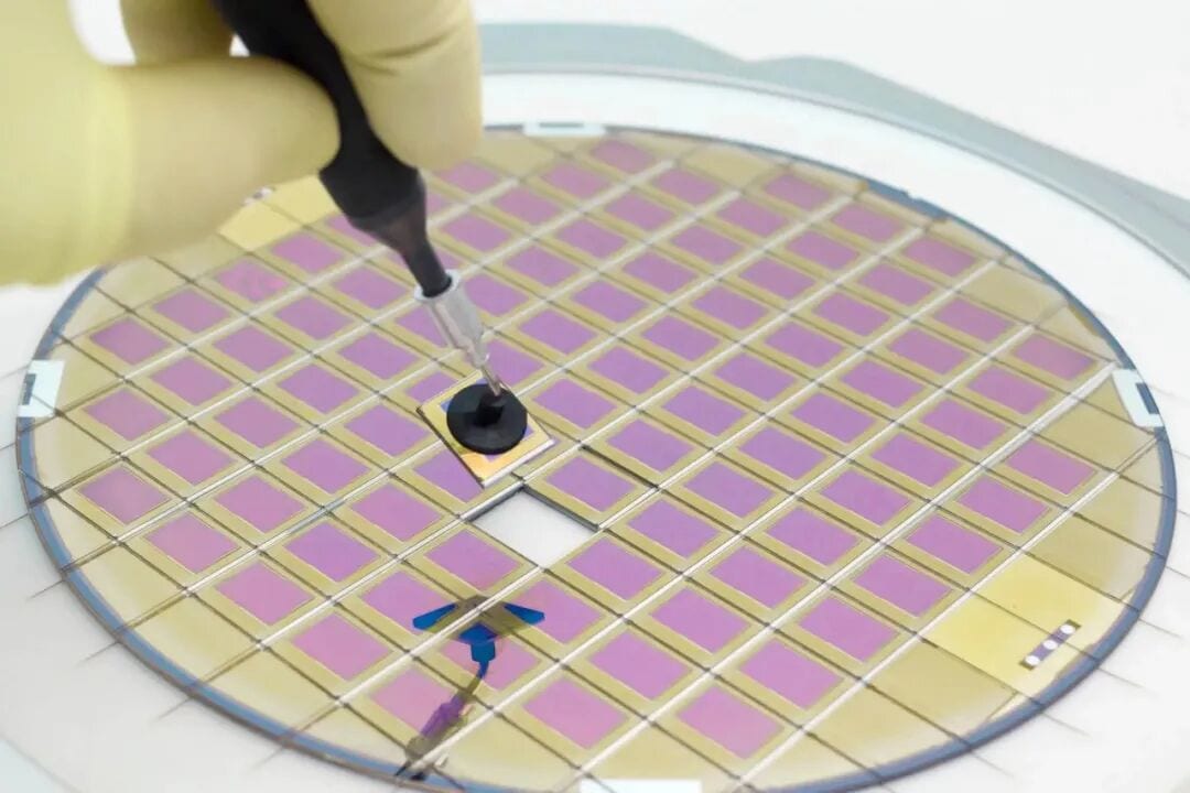
As mentioned earlier, a team from Westlake University proposed a batch method. The preprint describes it as a parallel gradient transfer process compatible with nanoimprint lithography, and demonstrates wafer-level patterning of four pairs of lenses on an 8-inch SiC wafer.
Put simply, a master template containing different grating parameters is made first, and these complex structures are then replicated in batches onto SiC through a process similar to imprinting and transfer.
In addition to the steps above, the finished waveguide must be assembled with optics, mechanics and other components into a complete display module, and the packaging itself may also affect the waveguide's optical performance.
Based on the principle of total internal reflection, whether light can propagate stably inside the waveguide depends on the refractive index difference between the waveguide material and the external medium. The outside of a bare waveguide is usually air, but once it is built into a module, if an adhesive layer, protective layer or other optical material is bonded to the lens surface, the refractive index conditions at the interface change, and some light that previously propagated by total internal reflection may leak out.
It seems AR still has a long way to go before it can put SiC to use.
From raw materials to optical waveguides: where does SiC sit in the supply chain?
As we have repeatedly noted, SiC is not a new material in the supply chain. What is genuinely newer is "optical-grade SiC" for AR, but overall, production of the material itself has scaled up fairly quickly.
Companies overseas such as Wolfspeed and Coherent, as well as domestic players including SICC and TankeBlue, already have mature SiC crystal growth and wafer processing capabilities.
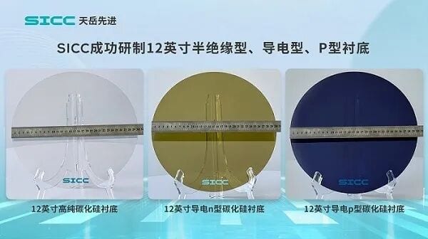
Among them, SICC Advanced is the fastest-moving domestic player. On March 26, 2025, at SEMICON China 2025 in Shanghai, it unveiled 12-inch high-purity semi-insulating and p-type silicon carbide substrates. In its half-year report released that July, SICC Advanced announced a strategic partnership with Sunny Optical Aolai, in which the former supplies materials expertise and the latter provides micro- and nano-optical processing capabilities, extending further into downstream optical devices.
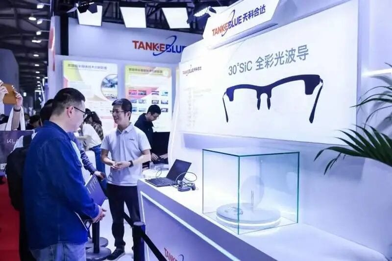
TankeBlue followed a similar pattern. At the same conference and on the same day, it unveiled its 8-inch optical waveguide SiC substrate for the first time and explicitly stated its intention to move it into volume production. A month earlier, TankeBlue and Mude Weina had formed a joint venture, with the former supplying SiC substrates and the latter handling micro-nano optics and diffractive optical waveguide processing. By 2026, its 8-inch optical waveguide substrate was being showcased as a standalone product.
Several established overseas SiC suppliers are also moving forward. Wolfspeed officially launched 8-inch SiC materials commercially in 2025 and produced 12-inch single-crystal SiC wafers in 2026. Coherent likewise already has the capability to produce 8-inch SiC substrates and epitaxial wafers, and announced a 12-inch SiC platform at the end of 2025. Unlike suppliers that only provide wafer materials, Coherent also has capabilities in diffractive couplers, optical coatings and more, so it has been working to extend SiC from a material into AR optical components.
In waveguide applications, many domestic companies are also making targeted investments and following up.
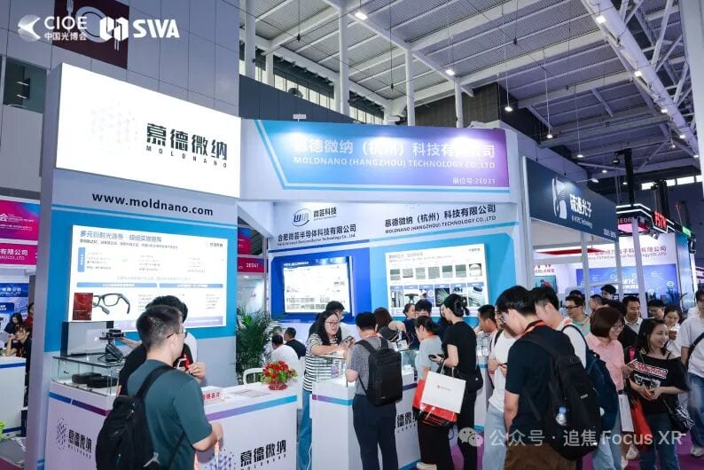
Mude Weina unveiled a SiC AR diffractive optical waveguide in 2024, and has since worked with a Westlake University team to advance single-layer full-color, rainbow-free solutions. At the end of 2025, its phase-one AR waveguide production line was completed, with officially disclosed nanoimprint and etching capacity reaching 5,000 8-inch wafers per month. By 2026, it demonstrated 30° and 50° full-color SiC waveguides; the 50° version was disclosed to achieve an optical efficiency of more than 1,000 nits/lm, and a system brightness of more than 3,000 nits in a demonstration paired with an optical engine. The 0.35mm waveguide mentioned at the beginning also comes from this industry-academia-research system.
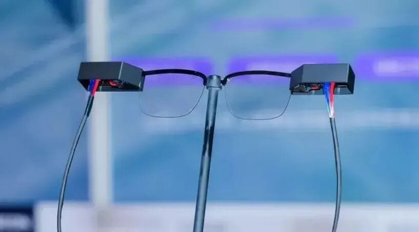
Guangna Siwei announced the C45C full-color SiC etched waveguide in 2025, with a thickness of about 0.7mm and a 30° field of view, and applied it in the Coray Air2 AR glasses. The company said the model has entered mass production and disclosed that several SiC full-color waveguides have been delivered in volume.
Goertek Optics has chosen a different route, focusing on a large FOV. In early 2026, Goertek Optics announced the F50Se full-color SiC optical waveguide display module, pushing the field of view to 50°. The F30Se SiC etched waveguide shown at the same time has been slimmed down to 0.65mm in thickness.
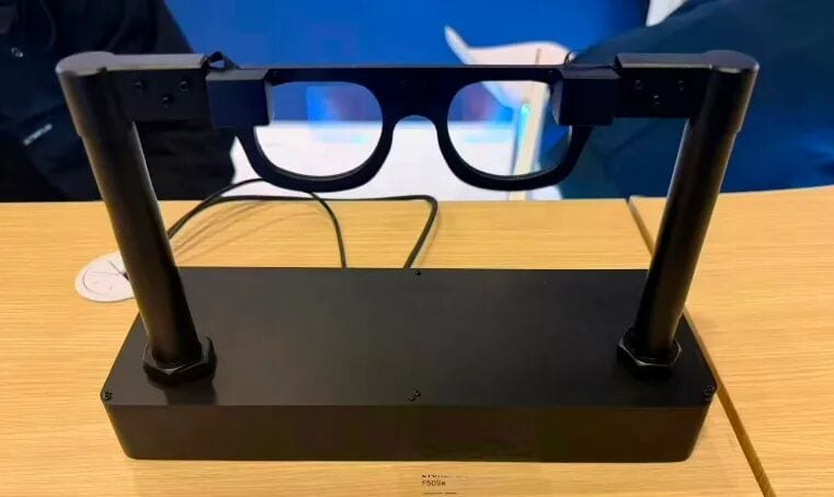
Sunny has also included SiC in its next-generation AR optics solutions. In its public materials, the target for the SiC optical waveguide solution is a field of view of more than 50°, and the company is cooperating with SICC on the material side.
At present, the materials side is relatively mature, building on established capabilities. Both 8-inch and 12-inch platforms are moving toward industrialization, while waveguide fabrication has reached wafer-level manufacturing, small-volume production and even end-product demonstrations. However, the industry still has a considerable way to go before achieving low-cost, high-volume consumer shipments, widespread consumer applications and broad market awareness.
Original title : The Next-Generation Material for AR Optics: Silicon Carbide Enters the Mass-Production Race
Source: OFweek Optics Network · News · optics.ofweek.com