SIOM and Partners Make Progress in Chip Effects Under Nanosecond High-Current Laser Proton Beam Irradiation
Topics and contents
SIOM, the Institute of Microelectronics of the Chinese Academy of Sciences, and ShanghaiTech University found that nanosecond high-current laser proton beams can enhance bit-flip effects in SRAM chips. The experiment produced a proton beam with a central energy of about 8 MeV and a pulse width of 2.3 ns. Bit-flip cross sections of 130 nm and 180 nm SOI-process chips were 2.2 to 3.8 times higher than those measured in low-flux tests with conventional accelerators. Combined Geant4 and TCAD simulations revealed the temporal-buildup enhancement mechanism from continuous proton charge deposition. The results were published in Applied Physics Reviews.
The study applies laser-driven nanosecond proton beams to chip irradiation, revealing how temporal charge buildup at high current affects bit-flip probability and providing an experimental path for extreme radiation-effects research.
SIOM Achieves Major Progress in Studying Chip Effects of Nanosecond High-Current Laser-Driven Proton Beam Irradiation
Recently, the State Key Laboratory of Ultra-Intense Laser Science and Technology at the Shanghai Institute of Optics and Fine Mechanics (SIOM), Chinese Academy of Sciences, in collaboration with the Institute of Microelectronics of the Chinese Academy of Sciences and ShanghaiTech University, made important progress in research on chip effects under nanosecond high-current laser-driven proton beam irradiation. The related results, titled "Upsetting SRAM units with laser-driven nanosecond proton flash", were published in Applied Physics Reviews.
High-energy radiation particles can alter the logic states of electronic chips, cause functional disruption and even failure. Current research on the damage mechanisms of chips and devices relies mainly on conventional accelerators, which have relatively low beam currents and pulse widths above the microsecond level. Proton beams driven by ultra-short, ultra-intense lasers inherently feature short pulses and high current, offering a completely new approach to studying ultrafast dynamic effects in chips and devices under extreme radiation conditions.
Relying on SIOM's petawatt femtosecond laser facility, the research team accelerated a proton beam through the interaction of an intense laser with a micrometer-thick aluminum foil. After energy selection and focusing by a magnetic quadrupole (PMQ) system, a quasi-monoenergetic proton beam with a central energy of about 8 MeV and a pulse width of 2.3 nanoseconds was obtained at the chip irradiation position, with an instantaneous flux as high as 5.5×10¹⁷ ions/cm2/s, about ten orders of magnitude higher than that of conventional accelerators.Irradiation experiments on 130 nm and 180 nm SOI process SRAM chips showed that, under irradiation by the laser-driven nanosecond proton beam with ultra-high current, the chip bit-flip cross-section increased by 2.2-3.8 times compared with low-flux test results from conventional accelerators, reaching a maximum of 10-13 cm2/bit.
Combined Geant4 and TCAD simulations by the team further revealed the "temporal pile-up" enhancement mechanism: when the arrival time interval of successive protons at the same sensitive cell is shortened to within a few hundred picoseconds, the carriers generated by the preceding protons have not yet been fully collected and recombined, and the charge deposition of subsequent protons continues to accumulate, significantly enhancing the transient current and progressively raising the storage node voltage until the upset threshold is exceeded, greatly increasing the bit-flip probability.
This work verified for the first time the nonlinear radiation effects excited by nanosecond high-current laser-driven proton beams in principle, providing a new approach for studying the ultrafast dynamics of silicon-based devices under extreme radiation conditions. It has important application prospects in device response to transient radiation generated by laser fusion and in simulating extreme astrophysical radiation events such as solar flares.
This work was supported by the Chinese Academy of Sciences Pioneer B Special Program, the Basic Science Centers Program of the National Natural Science Foundation of China, the Young Scientists Program of the National Key Research and Development Program, the Shanghai Rising-Star Program, the CAS Young Team for Basic Research with Stable Support, and the Shanghai Eastern Talent Program, among others.
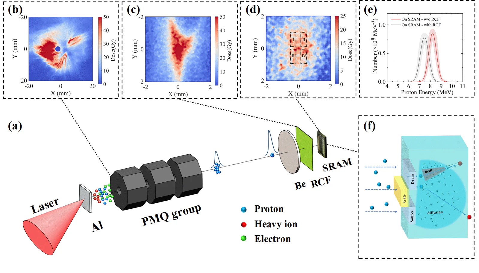
Figure 1 (a) Schematic of the experimental setup. (b)-(d) Spatial distributions of the proton beam behind the target, at the focal plane, and at the chip irradiation position; (e) Proton energy spectrum at the chip; (f) Schematic of electron-hole pair generation, drift, and diffusion in the MOS transistors of an SRAM chip under high-flux nanosecond proton irradiation.
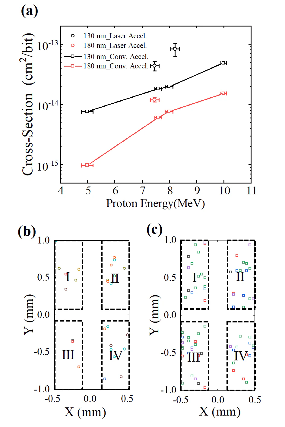
Figure 2 (a) Comparison of SRAM chip upset cross sections measured with a laser-driven proton source and a conventional accelerator; (b)-(c) Spatial distributions of upset locations in the memory array of a 130 nm chip under the two irradiation conditions.
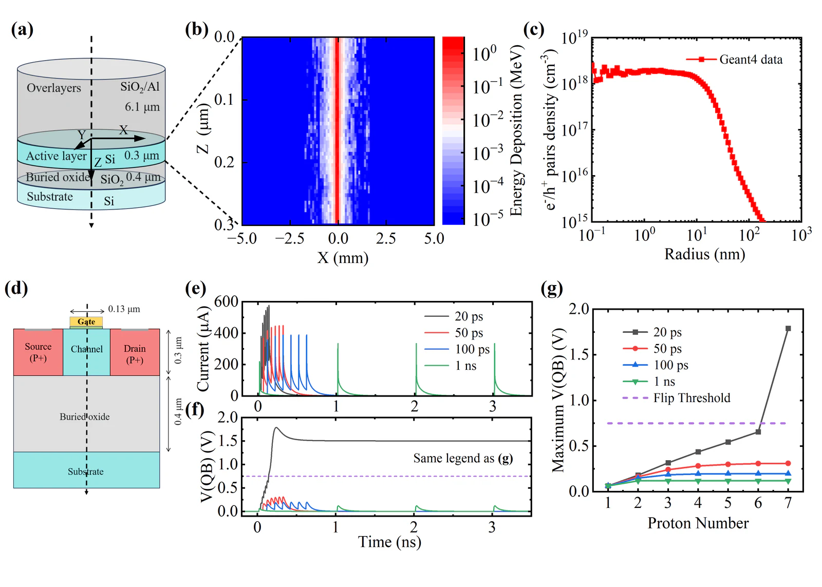
Figure3 Geant4andTCADsimulation results.(a) SOIchip structure in theGeant4simulation;(b) total energy deposition distribution in theX–Zplane atY=0after 10⁵protons are incident on and pass through the sensitive layer;(c) lateral distribution of the electron-hole pair density generated by a single proton passing through the sensitive layer, averaged over depth;(d) TCADschematic of thePMOSstructure in the simulation (proton incident at the center of thePMOSchannel);(e) transient currents induced by seven protons striking in succession at different time intervals;(f) transient evolution of the correspondingSRAMstorage node voltageV(QB)(initial value0 V);(g) peak node voltageV(QB)caused by successive proton strikes at different time intervals.
Source: Shanghai Institute of Optics and Fine Mechanics (SIOM) · Research Updates · siom.cas.cn